BANDF AD

NEO Semiconductor’s POC says 3D DRAM is good to go
Taiwan-based 3D X-DRAM developer NEO Semiconductor has had a successful proof of concept for its chips with strategic funding led by Acer founder and former CEO Stan Shih.
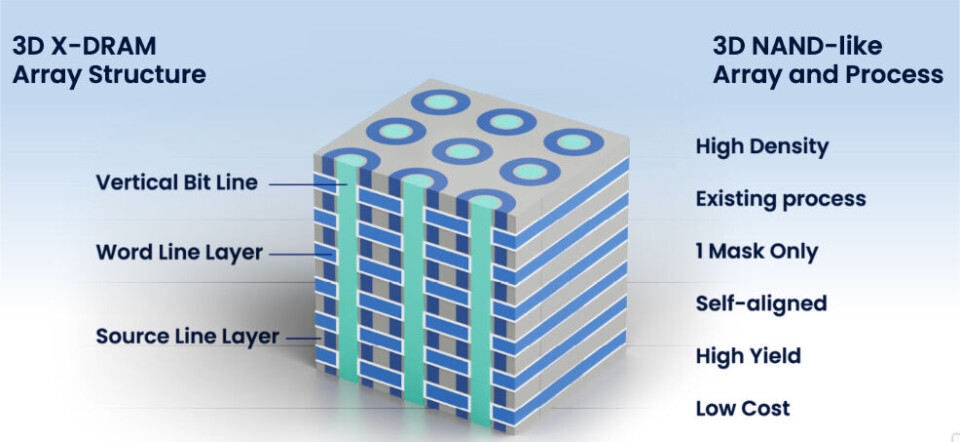
3D X-RAM builds layers of DRAM on a chip, like 3D NAND, combining the performance of planer, 2D DRAM with the manufacturability of NAND and a density roadmap of up to 512 Gb and beyond. Fabless NEO says it can provide 8 times more capacity for High Bandwidth Memory (HBM), meaning HBM capacity for GU server chips can be increased from 192 GB to 1.5 TB, resulting in a boosted performance for AI applications and much lower KV Cache pressure. HBM is currently in extreme high-demand with sustained price increases and supply shortages.

Andy Hsu, Founder and CEO of NEO Semiconductor, said: “We believe this technology can enable significantly higher density, lower cost, and improved energy efficiency for the AI era. By leveraging established 3D NAND manufacturing processes and ecosystem, we aim to bring 3D DRAM to reality sooner. NEO is actively engaging with leading global memory and semiconductor companies on potential co-development opportunities, and we believe our technology is well suited for a scalable licensing and partnership model to bring next-generation AI memory solutions to market.”
BANDF AD
The POC was developed in collaboration with National Yang Ming Chiao Tung University (NYCU) in Taiwan, specifically its Industry-Academia Innovation School (IAIS), and was fabricated and tested at the National Institutes of Applied Research- Taiwan Semiconductor Research Institute (NIAR-TSRI). POC test chips demonstrate that 3D X-DRAM can be manufactured using existing 3D NAND infrastructure, including established equipment, materials, and processes. The device successfully passed extensive electrical and reliability evaluations, confirming the robustness and stability of the proposed memory architecture.
POC results include:
• Read/write latency: <10 ns (DRAM c 10-20+ns)
BANDF AD
• Data retention: >1 second at 85°C (15× better than the 64 ms JEDEC DRAM standard)
• Bit-line disturbance: >1 second at 85°C (better than DRAM)
• Word-line disturbance: >1 second at 85°C (better than DRAM)
• Endurance: >10¹⁴ cycles (matches DRAM)
BANDF AD
Following this POC validation, NEO aims to develop 3D X-DRAM as a foundational technology for next-generation AI memory systems. It’s currently in active discussions with industry partners across the memory and semiconductor ecosystem to advance the technology toward commercialization.

The Stan Shih-led investor group funding supported the POC and will continue through the company’s next phase, including array-level implementation, multi-layer test chip development, and deeper engagement with leading memory companies to explore strategic partnerships.
Stan Shih said: “NEO’s 3D DRAM is expected to play a key role in future system architectures. As next-generation memory becomes increasingly critical to AI computing, innovations like 3D X-DRAM have the potential to contribute significantly to the evolution of the global memory industry.”
Andy Hsu, will deliver a keynote presentation at FMS: Future of Memory and Storage conference, August 4-6, 2026, at the Santa Clara Convention Center in California, USA, where he will discuss the company’s 3D X-DRAM technology and POC results, including performance and reliability metrics.